
Abstract
Graphene-Ceramic Composites (GCCs) have been little studied compared to graphene-polymer composites 1. Recent reviews 2, 3 indicate that both mechanical and electrical property ceramic improvements can be obtained by mixing small quantities, typically 1 to 15% of graphene material with a ceramic precursor, then compacting and sintering. The greatest effect is on the electrical properties. The electrical conductivity of a material was first shown to rise by several orders of magnitude for only a 1% volume addition of graphene as in polymer composites 4 but the stiffness, strength and toughness only increased by 20-160% or so at 5% addition, a rather minor improvement compared to significant increases caused by slight ceramic process changes. Some crack bridging and pull-out mechanism was observed by electron microscopy in graphene-alumina composites, though the effects were modest. Surface friction and wear improvements of around 100% were also notable. This paper seeks to show that much higher toughness increases might be produced using the method pioneered by Clegg et al 5, where the graphite interlayers are replaced with graphene to produce improved ordered interfaces with reliable coverage and consistent interface fracture energy, enabling an increase in the fracture resistance of the ceramic by two orders of magnitude.
Author Contributions
Academic Editor: HUANG Haitao, Applied Physics Department, Hong Kong Poly
Checked for plagiarism: Yes
Review by: Single-blind
Copyright © 2018 Bill Clegg, et al.
 This is an open-access article distributed under the terms of the Creative Commons Attribution License, which permits unrestricted use, distribution, and reproduction in any medium, provided the original author and source are credited.
Competing interests
The authors have declared that no competing interests exist.
Citation:
Introduction:
The search for tough ceramic materials accelerated during the past century, with surges in discovery during both the fiber period (1932-1970), the phase transformation decades (1970-1990) and the laminate era (1990-now). Before these exciting inventions in our lifetimes, ceramics were always brittle and failed alarmingly on scratching or impact.
The invention of tempered glass around 1874 led to the mistaken idea that ceramics could be ‘toughened’ by heat treatment. In reality, this tempering effect was produced by compressive residual stress in a heat-treated glass surface giving a higher fracture stress, not a higher energy. Tempered glass is still just as brittle as ordinary glass, dramatically illustrated when a scratch or crack goes through and past the outer compressed layer to cause explosive shattering. Bullet-proof glass (laminated glass) could be more properly called tough, because the polymer layers bonding the glass sheets together do inhibit cracking and increase the energy to failure. But this material is less than 90% glass because of the polymer interlayers, so is not truly ceramic. The concept outlined here is one where the polymer interlayers in bullet-proof glass are replaced by controlled ceramic interfaces, made with nanoparticles like graphene. Previous work has shown that it is essential that any such film should be continuous with no gaps to allow crack escape into the underlying ceramic.
By toughness, we mean an increase in energy dissipation, that is an increase in the resistance to fracture, R, when cracks attempt to run catastrophically through the material. Energy dissipation slows down the crack, producing stable or graceful collapse as opposed to dangerous, explosive shattering. The fibre toughening effect occurs because the crack is made to cross many interfaces between fibres and matrix, with certain types of interface giving substantial energy loss. This principle has been known since the invention of Fiber (asbestos) Reinforced Polymer (FRP) in 1905 by Leo Baekeland followed by much development in the 1920s and 30s. Cementing fibers together with thermosetting resins gave composite materials with a superb blend of properties: stiffer, stronger, tougher than each individual component. The downsides were the softness, temperature intolerance and water sensitivity of the products.
Fiber toughened ceramics are best exemplified by carbon-carbon composites, because these have wide application in aircraft and racing car brakes, but also in spacecraft nose-cones and rocket nozzles. Although cement bonded steel mesh, invented in the 1870s can be partly viewed as a ceramic composite with enhanced toughness, it is porous, water sensitive, functioning at low temperatures. Carbon fibers were discovered in the 1950s and began to be used in Fibre Reinforced Polymers (FRPs). When such materials were accidentally baked in an inert atmosphere in 1958, the resin matrix pyrolysed to carbon to produce a carbon-carbon composite with interesting strength and toughness properties 6, 7. But the difference between polymer-composites and ceramic composites is the large sintering shrinkage during ceramic manufacture. The reinforcing fibres cannot accommodate such shrinkage strains. Now, newly developed matrix processes, including shrink-free chemical vapor deposition of the carbon, give more high-quality carbon-carbon composites for technical applications 8 but at very much greater processing costs.
Transformation toughening is exemplified by the performance of partially stabilised zirconia eg 3YSZ (3%mol Yttria Stabilised Zirconia) described by Garvie and colleagues in the early 70s 9, 10. Analysis of cracks moving through this metastable material showed that energy was dissipated at the crack tip due to the change in structure and 3% volume expansion of the partially stabilised zirconia crystals under the intense crack tip conditions. An order of magnitude increase of fracture energy was possible from this mechanism.
In the invented process for tough ceramics dating back to the 90s 5, 11 sintering of laminated ceramic tapes coated with controlled interface material produced a laminated structure to deflect cracks Polymer processed silicon carbide powder tapes were painted with a graphite nanoparticle interface layer, then cold pressed in a stack before sintering under normal furnace environments. When notched and bend tested as in Figure 1, the crack was seen to be deflected such that the energy dissipated rose from 28 to 6152 Jm-2, with K1c of 20 MPm-1/2. This improvement is larger than that seen both in carbon/carbon composites and in transformation toughened zirconia, as shown in Table 1. Failure was not catastrophic while the failure stress rose by a factor 3 after the initial crack propagation from the notch. However, the graphite interphase structure was not optimised. The interfaces could most likely be much improved by moving towards graphene as a precise controllable interface within the ceramic composite. Layered structure is one of the few examples in which both toughness and strength can be increased simultaneously.
Figure 1.Bend testing a notched silicon carbide laminated composite, showing the crack deflexion
Table 1 compares the three types of ceramic composite. It is illuminating because it shows that, although carbon-carbon composites give a substantial toughening effect, such materials require a lengthy, expensive process that is currently viable only in aerospace and racing car applications, while the simpler ceramic powder processes can offer comparable or better toughness for everyday economic products.
Table 1. Improvement in energy to fracture of ceramic composites where G2 is the composite fracture energy and G is the fracture energy of the monolithic ceramic| Type of composite | Factor of toughening G2/G | Comments |
| Carbon-carbon composites | 60 | expensive CVD process |
| Transformation toughened 3YSZ | 30 | simple powder process |
| Laminated ceramic | 220 | simple powder process |
The purpose of this paper is first to postulate that the interfaces in the ceramic composite are vitally important in controlling the crack retardation, then show how nanoparticle graphene interfaces might be used to form more continuous, smooth and controllable interfaces in laminated ceramic composites.
Definition of Fracture at Interfaces
It is important to clarify the theory of interface fracture because confusion about interface cracking persists through the misleading concept of ‘interface strength’ 12. This has arisen through the largely empirical development of FRPs over the last century, when it was convenient to indent, stretch, bend or shear a composite test sample, observe damage, measure a force, divide by an arbitrary area to give a number with the units of a stress which could be standardised to a certain extent. But it was shown by Griffith 13 almost a century ago, when he demonstrated that the force to propagate a crack within an infinite sheet under uniform tension depends on dimensions of length3/2 not on length2.
Cracking depends very much on the geometry of the test piece and on the direction of propagation, so that the force required for cracking can depend on crack length in different ways 14. The simplest crack is observed in adhesive peeling shown in Figure 2a. The force F to propagate the peel crack at equilibrium is given by
F = bW/2 (1)
where b is the strip width and W the thermodynamic work of adhesion. The force F surprisingly does not depend on the area of contact of the strips.
Figure 2.a) Peeling crack; b) delamination crack
By changing the grip on the strips, (Figure 2b) the crack turns into a delamination or so-called ‘overlap joint’ configuration where the crack travels in the same direction as the applied force, strangely perpendicular to a Griffith crack. Applying the same fracture mechanics analysis to this arrangement gives the solution for force F at equilibrium 13
F= b(4WEd)1/2(2)
where W is interfacial work of adhesion, E Young’s modulus and d strip thickness. This equation has the same dimensions as the Griffith equation but the propagation force here does not change as the delamination proceeds, whereas the Griffith crack accelerates with crack extension.
In practice, observing cracks in thermodynamic equilibrium 15 is not straightforward and the fracture resistance, R, is often found to be several times greater than W. This is due to energy losses that can occur in the sample during cracking. These increase with both crack speed and temperature.
However, in peeling, cracking is stable. Plotting experimental results in Figure 3 for R, the real measured interface cracking energy, for both the peel and delamination tests of Figure 2 show that equations 1 and 2 are valid but exhibit widely different fracture forces for the two geometries, while giving crack force dependence on speed of fracture 13.
Figure 3.Plots of crack line force results for two tests as function of crack speed showing increase of force with speed and higher force for delamination crack than for peeling. The lines are equations 1) and 2) with R replacing W.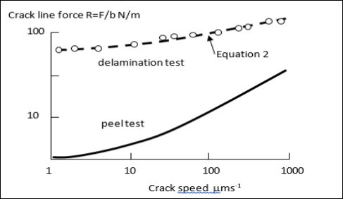
The most interesting feature of such an analysis is that equation 2 has similar dimensional form to the Griffith crack equation so that dividing equation 1 by equation 2 gives a simple number around 10 16 where Rc is the cohesive fracture energy for Griffith cracking, Ra is adhesive fracture energy of the delaminating interface and ν is Poisson’s ratio
Rc/Ra = 4π (1- ν2) (3)
In other words, the condition for a Griffith crack to be deflected at an adhesive interface is that the adhesive interface fracture energy must be about ten times less than the ceramic fracture energy. Interface strength cannot enter this theory.
These ideas are relevant to laminar interfaces in composites because they were used successfully in 5, 11 to interpret the results seen in ceramic laminate composites. But there are two other parameters to be taken into consideration. One is an elastic modulus change at the interface as the crack approaches 17. A crack finds it difficult to penetrate a higher modulus material. Effectively, the toughness can increase by a factor E2/ E1 as a crack moves from a low modulus component E1 into a high modulus region E213. The second parameter is crack healing and peeling as smooth crack surfaces are pulled back into contact by surface forces to form interfacial dislocations 18, 19, 20. When a smooth surface revealed by delamination heals in a new position, more energy must be dissipated to break the interface repeatedly, giving increased energy loss and therefore more toughness 13, as indicated by phenomena observed in fracture of nacre, which has a laminated structure with low interface fracture energy.
Graphene Interfaces
The major difficulty in this area is that very little is known about interfaces between ceramics and graphene and this is an area where significant further study is required. Measurements of the interface adhesion fracture energy, its dependencies on crack speed and temperature, the influence of the atoms attached to the graphene platelets, the effects of processing temperatures and environments; none of these are known or understood at present.
One exceptional paper appeared in 2010 from Wan’s group 21. A thesis from Li, one of his PhD students, puts the ideas in timely perspective 38. 50nm diameter gold nanoparticles were spread thinly on a (100) silicon wafer oxidised with a layer 280nm thick. Graphene sheets were mechanically cleaved from the surface of highly oriented pyrolytic graphite (HOPG-ZYH grade from NT-MDT Co., Moscow, Russia) using the celebrated method of Scotch tape peeling 22, 23. The tape carrying the adhered small flakes of graphite was then brought into contact with the Si substrate in dry condition, trapping a number of gold particles at the graphene-silicon interface. The thick silicon substrate suffered negligible deformation and was taken to be rigid, while the thin graphene sheet bent and formed a blister, in which the van der Waals forces pulling the graphene flake into contact with the wafer were balanced at equilibrium by the elastic reaction of the deformed flake. The measured interfacial adhesion energy R was calculated from the particle height and blister radius measured by scanning electron microscopy using the thin clamped membrane equation and energy balance crack equation 24
R = Eh (w/r)4 /16(4)
where E=0.5TPa was the elastic modulus of the graphene sheet, h=1.7nm its thickness, 5 layers, w the diameter of the gold particle and r the blister radius. R was found to be 0.151±0.028 Jm-2.
It is difficult to say how near this value of R=0.151 Jm-2 is to the equilibrium work of adhesion W. To understand that, and to see the effects of crack speed, it would be necessary to observe the peeling and healing of the graphene sheet on the wafer with time and environmental conditions, as was achieved with elastomeric materials many years ago 25. Of course, placing a graphite flake on a substrate under ordinary atmospheric and rough conditions is unlikely to give a realistic value of R = W, due to the presence on both surfaces of adsorbed chemical groups (Figure 4).21
Figure 4.a) SEM image of blister showing the central nanoparticle as a black spot; b) 3D schematic diagram of the blister; c) cross-section of the blister on the substrate with the central nanoparticle deforming the graphene platelet as an elastic membrane 21. Reproduced from Zong et al, J Appl Phys 107(2010)026104, with the permission of AIP Publishing.
Since 2010, several interesting papers have followed to consider the interfacial fracture energies of graphene in contact with oxide and other surfaces. Reference 26 was the first report of interface fracture energy for a large surface area graphene monolayer grown by CVD on copper. One interesting development was to consider a more standard interface fracture energy test than the blister method, which is not generally applicable to laminate systems. The double cantilever beam (DCB) method in contrast is widely favoured for laminates and has a long track-record for polymer composites 27. A target substrate was bonded with epoxy resin to the graphene surface (Figure 5)26 and bending cleavage forces applied. The value of R=0.72±.07 Jm-2 was determined under ambient room conditions. However, the velocity of the crack was not determined, and the dependence of R on speed and temperature is unknown. If epoxy resin had been used to form one of the cantilever arms, then the crack would have been visible and these parameters could have been observed as a function of temperature. Also, if the copper had been reacted to form oxide or other ceramic material, a measurement of a graphene-ceramic interface fracture resistance would be possible.
Figure 5.DCB test for measuring interface fracture energy of graphene to copper 26. reprinted with permission from Yoon, T. et al (2012) Nano Lett. 12, 1448-1452 copyright 2012 American Chemical Society.
Another step forward was the realisation that the interface fracture energy could increase significantly with the ceramic processing conditions 28. Using a nano-scratch adhesion measurement method, which is easy but unreliable, the as-transferred graphene adhered to SiO2 with R= 3Jm-2, a high value. But after rapid temperature rise and vacuum annealing, R rose to 10 and even 20Jm-2. The suggestion from XPS profiling was that C-O and C=O chemical bonds were forming at the interface to enhance the usual van der Waals interactions.
Most measurements of the fracture resistance of graphene interfaces have been made using the blister test 29, 30, 31, 32, 33, 34, 35, 36. This shows a range of features. Koenig et al. 29, 30 measured the adhesion of micromechanically exfoliated graphene on SiO2, obtaining 0.45 Jm-2 for monolayer graphene and 0.31Jm-2 for two to five layered graphene. Under nominally similar conditions, Boddeti et al. 31 found the adhesion energy for the graphene/silicon interface to be 0.250 Jm-2, which suggests some variability in these measurements.
Liechti’s group at University of Texas focussed on transferring a CVD grown graphene layer from copper to polished silicon wafers and polished copper surfaces with measured roughness 32, 33, 34, 35, 36. They measured R=0.34 Jm-2 at steady state but found interesting changes as mixed-mode cracking was introduced by changing the thickness of the polymer film used as backing for the graphene. They interpreted this effect in terms of surface asperity locking.
Interface fracture measurements on the as-grown CVD film gave higher values of R ranging from 0.74 to 1.53 Jm-2 depending on the copper surface treatment creating nano roughness 34, 35, 36. Rougher surfaces gave higher adhesion for CVD films whereas the transferred films gave lower adhesion at higher roughness. Such effects are well established in the adhesives industry where roughening a surface prior to setting the adhesive increases adhesion whereas pressure sensitive adhesion is reduced on roughened substrates. Transfer of graphene films may trap molecules or asperities which lower the adhesion, while further processing of the composite (eg by sintering) could increase the adhesion through annealing.
A more recent paper shows that there is a shear zone outside the blister edge, indicating sliding of one graphene sheet over the other. From the optically observed strains, a shear stress of 40 kPa could be calculated 37. This could be relevant to formation of interfacial dislocations in the displacing layers causing energy dissipation as a crack propagates. This is likely to depend significantly on the number of graphene layers in the sheet, allowing adhesion tuning. Gao et al 39 showed by blister testing that the R = 0.453 Jm-2 for monolayer, 0.317 Jm-2 for 3-5 layers and 0.276 Jm-2 for 10-15 layer graphene. Further recent analysis of blisters has continued 40 but the elastic processes analysed are much less significant than those arising from crack speed, temperature and irreversible loss effects, so may probably be neglected as academic hair splitting.
Mixing Graphene to Form Ceramic Composites
By far the most popular method for making ceramic composites has been that of mixing nanoparticles with the ceramic powder, then compacting, followed by spark sintering. Much previous study of carbon nanotube additions to ceramic powder processes 41, 42, 43, 44, 45, 46, 47, 48, 49, 50 had shown the potential for improving hardness, strength, toughness and other desirable characteristics. It was logical to try the same experiments using graphene additions. The advantage of graphene over nanotubes is to produce large, smooth and controlled interfaces in ceramic laminate materials, with easy dispersion and high toughness. Furthermore nanotubes are relatively short, so that their potential for crack bridging and increasing toughness is rather limited; graphene platelets can be more extended.
A further area where graphene may give benefits is that it can be introduced as a thicker interphase layer, that might itself be toughened. This would limit the extent of crack growth along the laminae, which in the early materials, could reach almost to the ends of the sample.
The review 51 in 2013 showed that encouraging property improvements were being achieved with graphene in various ceramic matrices, especially electrical properties shown in Figure 642, 51, 52, 64 The specific benefits were dependent on the graphene source and preparation, the mixing and compaction methods, then the sintering techniques. In this section we consider the bulk manufacturing processes. Then the next section deals with special processes for making functional ceramics, especially electrical components.
Figure 6.Increase in electrical conductivity (GO-YSZ) (GNP-Si3N4) (GNS alumina) FLG (Al2O3) [42, 51, 52, 64].![Increase in electrical conductivity (GO-YSZ) (GNP-Si3N4) (GNS alumina) FLG (Al2O3) [42, 51, 52, 64].](/article/773/images/image10.jpg)
Bulk ceramic composite investigations have largely used graphene made from graphite, either by mechanical delamination, by the Hummer chemical splitting method to form graphene oxide, or by the electrolytic method. The largest demand is for polymer composites 53 but the same graphene preparations will also be applicable to ceramic products. High shear exfoliation using new designs of machine plus ultrasonic treatment has been of great interest 54. Combined with the electrolytic method (figure 7)53 using chemical additives to get between the graphene layers 55, followed by centrifuging to separate the nanoparticles, high yields of around 20% have been demonstrated.
Figure 7.a) The electrolytic exfoliation of pure graphite; b) high shear mechanical splitting 53.
Hummers method produces graphene oxide which is highly defective and needs to be reduced to get the graphene flakes back to their original condition. To produce graphitic oxide using modified Hummer’s method, commercially available graphite powder is treated with sodium nitrate (NaNO3), sulphuric acid (H2SO4) and potassium permanganate (KMnO4) at 0oC for 2 h. After stirring the mixture for 30 min at room temperature, distilled water is slowly added while maintaining the temperature below 98oC for 3h. The mixture is subsequently treated with hydrogen peroxide (H2O2) followed by filtering and washing with distilled water. After dispersing the mixture in distilled water and ultasonicating for 15 min, the dispersion is centrifuged and stable supernatant containing GO is collected 56.
The earliest ceramic mixing method was ball milling the graphene, typically with N-Methyl Pyrrolidone (NMP) and/or alcohol as the fluid dispersant, then adding the ceramic powder, for example alumina, zirconia, silica or silicon nitride, followed by filter pressing to compact. Colloidal processing has also been successful, by mixing colloidal stable dispersions of the graphene and the ceramic particles. In a recent example, alumina powder was suspended drop by drop to produce a well dispersed mix which was castable by normal ceramic methods. Sol gel and polymer based ceramic methods have also been used to produce thin coatings or porous ceramics for lithium battery electrodes 51.
The main difficulty in processing the graphene ceramic composites is the sintering step. Pressureless sintering, as normally used in the bulk ceramics industry, takes too long at high temperature leading to degradation of the graphene plus large grain growth. Hot pressing and isostatic hot pressing have been used to produce dense samples quickly 57. The graphene addition to the ceramic matrixes varied from 1 wt.% to 2 wt.%. Graphene composites with Alumina were prepared using commercial powder: submicron aluminium oxide (0.1 μm, Taimicron TM-DAR of Taimei CHEMICALS CO., LTD) and nanometric graphene Gn(4) of Cheap Tubes, USA with following parameters: Colour: black, purity: 99 %, average flake thickness: 4 nm, average particle (lateral) size: 1–2 μm, specific surface area: >700 m2/g. The powder mixtures were homogenized for 10 h in propanol using a rotary-vibratory mill and alumina grinding media. Dried and granulated powders were hot-pressed (Thermal Technology LLC) at 1400 °C for 1 h under 25 MPa in argon flow. The heating rate was 10 °C/min to make 50mm samples.
Si3N4–graphene composites were made of commercial submicron silicon nitride (0.5–0.8 μm, Grade M11 of H.C. Starck) and the same nanometric graphene Gn(4). For the activation of the sintering, the aluminium nitride (0.8–1.8 μm, Grade C of H.C. Starck) and yttrium oxide (0.5–0.8 μm, Grade C of H.C. Starck) powders, with the 2.5 wt.% and 4 wt.% were used. The powder mixtures were homogenized for 6 h in propanol using a rotary-vibratory mill and silicon nitride grinding media. Dried and granulated powders were hot-pressed (Thermal Technology LLC) at 1750 °C for 1 h under 25 MPa in nitrogen flow. The heating rate was 10 °C/min making 50mm samples.
Spark plasma sintering has been the main innovation giving finer grains at shorter firing times. The composite mix, the punch and the die are both Joule heated at around 100K/min and pressing can give up to 1 GPa to sinter in a few minutes at relatively low temperature.
The properties of the graphene reinforced ceramics made by these methods were somewhat improved. Typically bending strength rose by 60% and indentation toughness K1c rose from 4 to 5 MPa m1/2 for alumina and from 5 to 6MPa m1/2 for Si3N4. Fracture surfaces showed that pull-out of the graphene flakes interfered with crack propagation. Electron microscopy showed excellent contact between graphene platelets and ceramic crystallites and crack deflection mechanisms (Figure 8)2. However, the measured toughnesses are still somewhat low, suggesting that the graphene layers are not continuous, possibly due to reaction with the underlying ceramic substrate, suggesting that layers need to be either thicker or substrates inert to graphene.
Figure 8.Electron microscope pictures showing graphene influencing cracks in the ceramic composite 2 reprinted with permission from Miranzo, P., Belmonte, M., Isabel Osendi, M., (eds) (2017) Graphene ceramic composites, J Euro Ceram Soc 37, 3647-3822.
Significant improvements were shown for SiC/graphene composites 58. Briefly, two separate suspensions using alcohol (ethanol or isopropyl alcohol) as liquid media were first prepared to disperse and homogenize their components, in particular, one attrition milled ceramic slurry with a powder composition formed by 93 wt.% of β-SiC powders (BF-17A, H.C. Starck GmbH) plus 5 wt.% of Y2O3 (Grade C, H.C. Starck) and 2 wt.% of Al2O3 (SM8, Baikowski Chimie), and another one containing the selected graphene fillers (GNPs or GOs) that was sonicated. Afterwards, both suspensions were blade mixed and sonicated, and the dried and sieved powders were spark plasma sintered (SPS, SPS-510CE, Fuji Electronic Industrial Co., Ltd.) at 1800 °C for 5 min, applying 50 MPa of uniaxial pressure and using a vacuum atmosphere of 6 Pa. Disc shaped specimens of approximately 20 mm diameter and 3 mm height were obtained. The different materials selected for this study were the reference monolithicSiC (“SiC”) and SiC composites containing 5, 10 and 20 vol.% of added GNPs (“5GNPs”, “10GNPs”, “20GNPs”), and a composite with 5 vol.% of reduced GOs (“5rGOs”). Hertzian contact tests were performed in air by indenting (Zhu 2.5, Zwick/Roell GmbH & Co.) 1 μm diamond polished and gold coated specimen surfaces with tungsten carbide (WC-6% Co) spheres of 1.25 and 2.50 mm of radius. The specimens were placed so that the basal plane of the graphene fillers was oriented parallel to the tested surface, i.e., perpendicular to the SPS pressing axis. the addition of GNPs to SiC led to a remarkable increment in the fracture toughness (from 3.2 to 5.9 MPam1/2) giving almost 4 times the fracture energy. The penalty was hardness reduction by 20 to 30%.
Systematic Design of Nanoparticle Interfaces to Improve Properties
Mixing graphene nanoparticles with ceramic powders, then sintering the products, has shown significant but not stunning property improvements. The challenge is to design laminated structures which can give better results than random mixing, as pioneered in 5. A recent embodiment of this idea is given by Belmonte et al 59. They were striving to obtain directional conductivity in a Si3N4 composite laminated with graphene layers 200nm thick across the whole sample area. 5 such layers were embedded as shown by dark lines in Figure 9b59. An additional benefit should be increased toughness as cracks were impeded at the graphene interfaces.
Figure 9.a) Test samples of Si3N4/graphene laminated composite; b) Edge view after cracking from the top, showing some crack deviation at the graphene layers (the scale bar should read 1mm); c) fracture surface bumps showing crack deviation near graphene layer; d) no sign of deviation on control Si3N4; e) Comparison of properties for Si3N4 control and Si3N/ Graphene oxide laminate; f) indentation cracking picture with plot of toughness increase with indentation load for graphene laminate; g) detail of crack deviation at graphene layer 59 reprinted with permission from Belmonte, M., Nistal, A., Cruz-Silva, R., Morelos-Gomez, A., Terrones, M., et al (2015) Advanced Electronic Mater. 1, 1500132.
The results were affected by the reaction of the silicon nitride with graphene to form silicon carbide, but the small volume fraction (0.03%) of added graphene oxide gave 16 orders of magnitude increase in electrical conductivity in the plane of the laminations. For random mixed graphene such an increase in electrical conduction would require 7.2% of such flakes. The toughness increase was only 15% rise in K1c which is marginal, presumably because the interfaces were not substantially deflecting the crack. By hardness measurement, the increase in K1c was up to 60% as the indentation proceeded.
Another paper using laminated and sintered ZrB2 mixed with graphene plus SiC/graphene layers was shown to give increased bending strength and fracture toughness, because the cracks were in this case inhibited by the layered structure of the pressed product after spark sintering 60. Figure 10 shows how strength went up by 200 to 500% and K1c rose from 2 to 6MPam1/2 and from 4 to 9.6 MPam1/2, rather impressive gains.
Figure 10.Bioinspired laminated strength and K1c increases for layered ZrB2 SiC mixes with graphene 60
Significant numbers of publications are appearing on use of graphene in electronic applications due to the remarkable electronic properties of graphene films. Such functional composite ceramics may prove to have interesting potentials. In a review 61 application benefits and drawbacks were discussed in relation to infrared (IR) devices, electro-optic (EO) devices, and field effect transistors (FET) for radio frequency (RF) applications. Graphene may provide interesting solutions for certain electronic applications such as the channel in a field effect transistor, since it can be doped electrostatically and has extremely high mobility allowing for quick response (high operating frequency). The replacement of Si by graphene for logic gates might be considered due to the high potential switching speed, however the absence of a band gap means that a relatively large bandgap would have to be induced through a variety of doping or other symmetry breaking mechanisms. Graphene has the highest mobility values measured in a material at room temperature making integration into fast response time devices such as a HEMT (high electron mobility transistors) for RF applications. It has been shown that although the integration of graphene is challenging due to mobility degradation from surface contamination and trapped states in the oxide dielectric that a graphene RF detector with an overall response frequency of 300Ghz may be achieved utilizing a three-terminal design on a SiC substrate with a channel length of 40nm.
Graphene use in optical devices is limited 60 due to the absorption of 2.3% of incident light per layer making graphene’s use for optical devices a trade-off between getting enough layer for good optical absorption and modulation versus restricting number of layers for fast carrier propagation. On its own graphene in not practical for use as a waveguide or modulator but when it is combined with already active materials it increases the performance of such devices thus an EO modulator utilizing a stacked graphene-BN capacitor along with a Si microcavity array displays the ability to modulate light at a rate of 1.2 GHz.
Graphene for IR detectors has shown some promising results utilizing graphene in thermal-based detection regimes since the photon-based absorption regimes all require inducing a bandgap adding complexity and reliability issues. The unique thermal-based properties of graphene either in a traditional bolometric type of device or one based upon current produced from the photoelectric effect allowed for the creation of a graphene IR detector with sensitivity to a 2.5THz (119μm) laser.
Another application for faster nano-electronics is using fluorinated graphene to facilitate germanium replacing slower silicon devices 62. Insulating fluorinated graphene can act as an efficient diffusion barrier layer to suppress the formation of the unstable interfacial oxide in Ge-based devices. The Ge-based device with the fluorinated graphene exhibits negligible capacitance versus voltage hysteresis, extremely low leakage, and superior equivalent oxide thickness compared to silicon.
The interface control needed for crack control may also be useful for electronic devices as shown by Jung et al 63. Considering each interface encountered during the fabrication of graphene devices, from the graphene/metal growth substrate to graphene/high-k gate dielectrics, it is important to control the interface structure and properties at the atomic level. For effective delamination and transfer of graphene, adhesion at the interface of the graphene/metal growth substrate or graphene/target substrate should be engineered by appropriate weakening or strengthening methods for those interfaces. In terms of graphene delamination using polymer adhesives or a carrier layer, questions remains about which functional groups in the polymer play a critical role to induce delamination of graphene. This should be investigated systematically by applying reagents having various functional groups to graphene delamination systems, in conjunction with an investigation of doping effects that might be induced from the chemical groups. After graphene is transferred onto a target substrate, interfacial issues arise from the atom-thickness of graphene and the surface-graphene interactions. Since the surface states of substrates significantly affect the overall electrical properties of graphene devices, as well as the cleavage properties, substrates with a chemically inert, dangling-bond-free flat surface as well as high surface phonon energy are highly demanded. Although h-BN is an ideal substrate in terms of realizing high performance graphene electronics, obtaining reliable, large-area synthesis methods for h-BN beyond mechanical exfoliation is still a challenging issue. On the other hand, alternative substrate materials, such as AlN, are attractive, as highlighted in 62. To deposit a high-k dielectric using ALD, it is necessary to introduce seed materials onto graphene due to the chemically inert surface of graphene or to generate seeding centers on graphene itself. These approaches cause heterogeneous dielectric stacks (or interfaces) and give rise to difficulty in controlling the film thickness, thereby constraining the scaling of gate dielectric thickness. A novel approach for the deposition of gate dielectrics therefore should be explored to achieve a single component gate dielectric that forms a homogeneous interface without the application of additive seed layers. One example would be the deposition of ultrathin (less than 10 nm) dielectrics by the initiated CVD method. The use of ultrathin dielectrics in graphene FETs would also be desirable for the development of flexible electronic devices. In summary, interface control is vital both for crack control and electronic applications. Several reviews have mechanical bias, but the electronic nature of the interface must be closely considered 64.
Conclusions and Forward View
Ceramics have been getting tougher over the past century as the mechanism of cracking processes around composite interfaces has begun to be understood. Carbon-carbon brake blocks and transformation toughened zirconia are striking examples of such advances. Now there is a movement towards graphene interfaces in ceramic composite materials and there is substantial progress in property improvement as graphene is added near 5% volume fraction.
Graphene at ceramic interfaces has already given improvements in ceramic properties, including modest toughness increases, simply by adding small volume fractions of nano-flakes to a ceramic powder formulation, compacting and sintering. The reason is that the graphene nanoparticles can make good contact with the ceramic crystallites and provide controlled smooth interfaces where energy dissipation can occur during fracture, inhibiting the failure process.
But the most exciting challenge is to produce graphene interfaces in laminated ceramic composite structures, such that fracture energy can be increased by several orders of magnitude, producing much tougher and more multifunctional products than seen hitherto. The realistic prospect is that graphene reinforced ceramic composites could achieve toughness near R= 10,000 Jm-2 and K1c = 20 MPam1/2 at low graphene volume fractions around 1%, together with the possibility of novel electronic properties stemming from the precise interface control.
Acknowledgements
Thanks are due to Dr Siva Bohm and Professor Andrea Ferrari at Cambridge Graphene Centre for discussing these points in a very positive way.
References
- 2.Miranzo P, Belmonte M, IsabelOsendi M, eds. (2017) . Graphene ceramic composites, J Euro Ceram Soc 37, 3647-3822.
- 3.Ramirez C, Wang Q, Belmonte M, Miranzo P, IsabelOsendi M. (2018) . , Scripta Materialia 149, 40-43.
- 9.Garvie R C. (1987) A personal history of the development of transformation toughened. PSZ ceramics, 4thInt Symp Sci and Technol of Sintering,Tokyo 239-250.
- 13.Kendall K. (2001) Molecular adhesion and its applications: the sticky universe,Kluwer Academic,New York,ch.15,16.
- 23.Novoselov S, Jiang D, Schedin F, Booth T J, VKhotkevich V. (2005) . , Proc. Natl. Acad. Sci. U.S.A 105, 10451.
- 27.Cho J U, Kinloch A, Blackman B, RodriguezSanchez F S, Han M S. (2012) . , International Journal of Automotive Technology 13, 1127-1131.
- 30.Koenig S P, Long R, Xiao J, Bunch J S, Dunn M L. (2013) . , J. Appl. Mech. Paper No:JAM-13-1043 80(040909), 1-8.
- 31.Boddeti N G, Koenig S P, Long R, Xiao J, Bunch J S et al. (2013) . , ASME J. Appl. Mech 80, 040909.
- 33.Cao Z. (2015) Mixed mode interactions between graphene and substrates by blister tests, PhD thesis U. Texas. 1-123.
- 38.Li G. NorthEastern University Boston Mass (2012) Thin film adhesion and morphology of graphene on undulated electronic substrates. PhD thesis
- 40.Harvey C M, Wang S, Yuan B, Thomson R C, Critchlow G W. (2018) . , Theor. Appl. Fract. Mech 94, 34-39.
- 57.Sedlak R, Kovalcikova A, Rutkowski P, Girman V, Dusza J. (2015) . , Powder Met. Process 15, 150-155.